Low damage etching of organic materials
2014.08.15 UpdateTOPICS
About Gas Cluster Ion Beams
Low damage etching of organic materials
Polyimide is widely used industrially for electronic materials including flexible substrates, liquid crystal display materials, semiconductor insulating films, etc. for its characteristics such as superior heat resistance and chemical resistance.
However, PMDA-ODA type polyimide cannot be etched with existing carbon cluster ions, making it unsuitable for practical analyses.
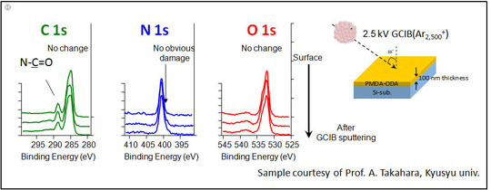
Figures 1 to 3 compare the XPS depth profile and spectral change when sputter etching is performed using 10 kV C60 and 2.5 kV Ar GCIB on polyimide film-formed at a thickness of 100 nm on Si. By using gas cluster ions, 100 nm polyimide film can be etched, enabling the quantitative value of XPS to be close to the value of the original chemical composition (Fig 1). In addition, the chemical state changes after sputtering with C60 (Fig 2), but with gas cluster ions, the chemical state does not change after sputtering (Fig 3).
So far, it has been shown that with gas clusters, depth profile analysis that does not change the chemical state can be performed easily even for organic materials, which was considered relatively difficult with carbon clusters such as C60, that layers damaged in the process can be removed, and deep sputter etching up to several dozen microns can be performed.
Fig 1, XPS depth profile when sputter etching is performed using 10 kV C60 and 2.5 kV Ar GCIB on PMDA-ODA thin film
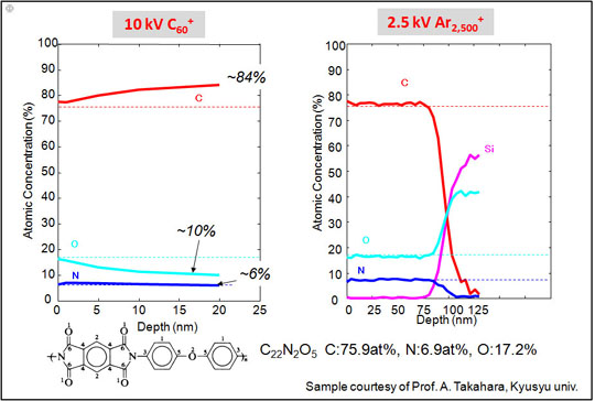
Fig 2, XPS spectral change when sputter etching is performed using 10 kV C60 on PMDA-ODA thin film
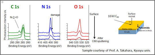
Fig 3, XPS spectral change when sputter etching is performed using 2.5 kV Ar GCIB on PMDA-ODA thin film