


Organic device analysis evaluation
2014.08.15 UpdateTOPICS
About Gas Cluster Ion Beams
Organic device analysis evaluation
In organic molecule devices such as organic light-emitting devices and dye sensitized solar cells, nanometer-level thin films play various functions, generating demand for unprecedented new surface features, interfacial features and more advanced performance in the last few years. In addition, advanced surface and interfacial features beyond those of existing materials are even demanded in areas such as electronic materials, which includes battery electrode materials (for fuel cells, lithium ion secondary batteries, etc.), electronic parts, and FPD. However, many such materials are easily damaged by irradiation of energy particles, and it is difficult to conduct depth profile surface analysis of their thin-film material, which is essential for evaluating surface and interfacial features.
This was a significant barrier for the development of stable material design. With XPS and TOF-SIMS, which are equipped with GCIB ion guns (proven to have low damage to organic materials), a low damage technology for depth profile analysis of organic molecular materials was realized. Sophisticated surface/interfacial material design for organic molecular materials is possible using this surface analyzer.
Fig 1 to 3 show the depth profile results from XPS and TOF-SIMS for an organic solar cell device created as a model.
Fig 1 shows a comparison of the results from a depth profile analysis at an acceleration voltage of 250 V with an Ar ion gun, an ion source commonly used in the past, and from a depth profile analysis performed using approximately 2500 Ar cluster ions at an acceleration voltage of 5 kV. Using an ion gun based on older technology at a low acceleration voltage to perform depth profile analysis will not result in much information regarding the chemical state. It will only detect marginal peaks in the vicinity of the interface derived from the sulfone group. On the other hand, depth profile analysis using the Ar GCIB shows that the two layers with different amounts of oxygen and chemical states are able to be analyzed separately.
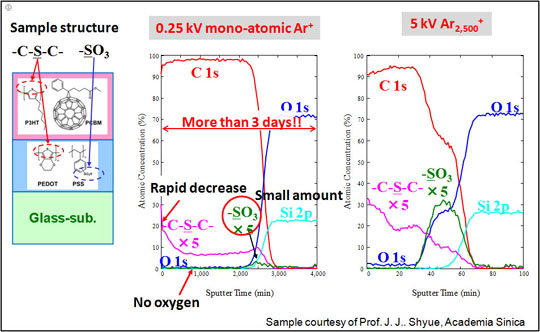
Fig 1, Comparison of XPS depth profiles by Ar and Ar GCIB of model organic solar cell sample
Fig 2 shows a comparison of the XPS depth profiles after heat treatment of the model organic solar cell device sample shown in Fig 1.
It clearly shows that with GCIB etching, the interfaces of the two layers became steep after heating.
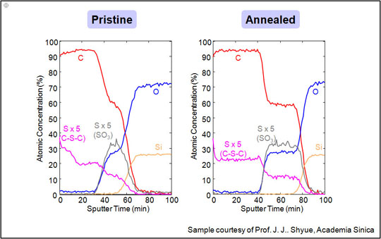
Fig 2, XPS depth profile of model organic solar cell sample
Fig 3 shows the TOF-SIMS depth profile of the same sample.
It shows that with TOF-SIMS, depth profile distribution in the film for a molecular ion with a mass number of approximately 900 is achieved.
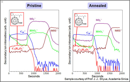
Fig 3, Negative ion TOF-SIMS depth profile of model organic solar cell sample