What is XPS?
What is XPS?
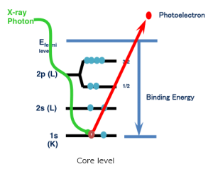
Principle
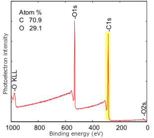
X-ray Photoelectron Spectroscopy (XPS) or Electron Spectroscopy for Chemical Analysis (ESCA) is a technique which analyzes the elements constituting the sample surface, its composition, and chemical bonding state by irradiating x-rays on the sample surface, and measuring the kinetic energy of the photoelectrons emitted from the sample surface. XPS instrument using Al Kα rays can generally obtain information on elements within a few nms of the sample surface.
Additionally, the change in bond energy (chemical shift) caused by the electron state surrounding the atoms to be analyzed, such as atomic valence charges and interatomic distances, tend to be greater than the chemical shift observed in AES, which makes the relative ease with which the state of chemical bonds can be identified another advantage of XPS.
 |
 |
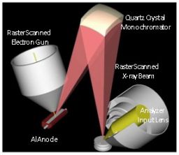
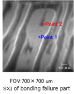
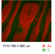
Excitation source (scanning micro-focus x-ray source)
A scanning micro-focus x-ray source is an x-ray source that can scan a focused monochromed Al Kα beam on the sample. In general, characteristic x-rays such as Al Kα rays and Mg Kα rays are widely used as excitation sources for photoelectrons. The x-ray beam diameter can be set between several µmφ to several hundred µmφ, and the scan range can be changed arbitrarily, enabling measurement of the most appropriate analysis area for the sample. Secondary electron image observation (SXI: Scanning X-ray Image) based on this feature also allows for quick and accurate analysis location designation. Additionally, it supports various analyses including multi-point simultaneous analysis, large area measurement, line analysis, and area analysis.
 |
 |
 |
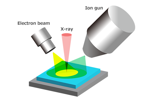
Charge compensation mechanism (dual beam charge neutralization)
XPS is used for element/chemical state analysis for a wide range of solid samples from conductive to insulating materials. However, with insulating material samples, a positive charge occurs in the x-ray irradiated area due to the generation of photoelectrons. A spectrum measured in a positively charged state shifts to the high bond energy side (low kinetic energy side) compared to its actual position, making it difficult to grasp the correct energy position. Thus, with insulating material samples, charge neutralization is necessary during measurement. The dual beam technique, which irradiates a low energy electron beam and an ion beam simultaneously, is a neutralization method which stabilizes uneven charges on the surface in a self-repairing way, and is capable of stable charge neutralization for a wide range of insulating materials. It is also an essential feature for microscopic area analysis.
Sputter ion gun (argon ion gun, cluster ion gun)
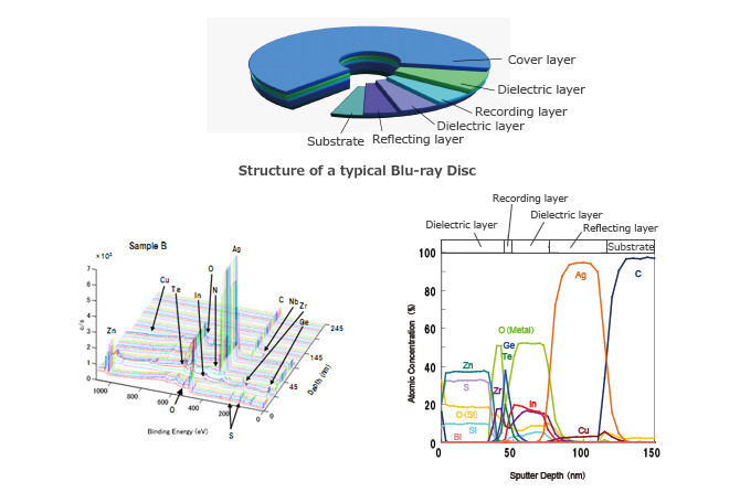
Since the information depth measurable with XPS is in the range of several nms from the surface, when the surface contamination layer is thick, or when evaluating a deeper area, ion sputtering is used to perform surface etching. An element composition or chemical bonding state depth profile can be obtained from the spectrum information gained through alternating between sputtering and measurement. Depth profiles are used for film thickness evaluation of samples with a multilayer structure and cause analysis for discoloration/corrosion of metal. Generally, argon (Ar) ions are used for depth profile analysis for inorganic materials such as metals and semiconductors while fullerene (C60) and argon gas cluster ions (Ar-GCIB) are used for organic materials, so different sputter ion guns are used depending on the material and purpose.