Semiconductor chips consist of a series of thin films that have been patterned to produce electronic devices. The use of surface analysis instruments to characterize the composition of thin films or patterned structures and detect contaminants or process residues is critical to the development of new materials, manufacturing processes, and increasing product yield.
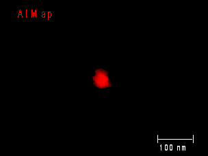
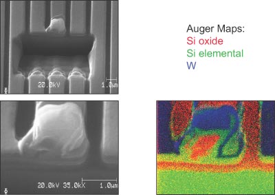
Defect Identification (AES)
The ability to identify the composition of nano-scale defects and determine their source of origin is critical to enhancing device yield. The continued shrinking of device size and critical defect size has limited the usefulness of optical methods and EDX analysis for sourcing ultra thin and ultra small defects. The PHI 700 Auger Nanoprobe is ideally suited for this application.
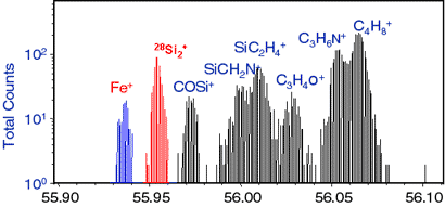
Trace Metal Contamination (TOF-SIMS)
Low level metal contaminants can have a serious impact on semiconductor device performance. The Patented TRIFT analyzer used in PHI’s TOF-SIMS surface analysis instruments provides a low spectral background and high mass resolution to provide the highest sensitivity and confident identification of trace level metal contaminants.
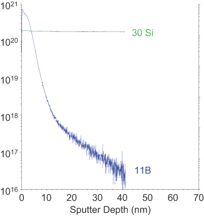
Ultra Shallow Implant Depth Profiling (D-SIMS)
Ultra Shallow implants are routinely used to create junctions for today’s high performance devices. PHI’s dynamic SIMS surface analysis instrument, the ADEPT-1010, provides a stable automated measurement platform for monitoring shallow implant processes.
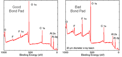
Bond Pad Surface Composition (XPS)
The composition and chemistry of bond pad surfaces influences device lifetime, physical, and electrical properties. For this reason many manufacturers of semiconductor devices monitor bond pad composition with PHI’s Quantera XPS surface analysis instrument. The Quantera provides high sensitivity micro-area XPS spectroscopy capabilities for monitoring the composition of small patterned features such as bond pads.