Analysis Examples
Measurement of occupied and unoccupied states of the same sample
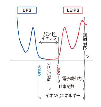
The overall picture of the band structure can be obtained from the energy of the unoccupied states measured by LEIPS and the energy of the occupied states measured by UPS (Ultraviolet Photoelectron Spectroscopy). By combining LEIPS and UPS in a complementary manner, both the electron and hole levels of semiconductor samples can be determined.
Furthermore, the electron affinity can be obtained from the lowest unoccupied molecular orbital (LUMO) measured by LEIPS, and the ionization energy can be obtained from the highest occupied molecular orbital (HOMO) measured by UPS. The band gap of the semiconductor can be determined from the difference between these values.
Measurement of Electron Affinity
In LEIPS, the bandpass filter of the photodetector can be replaced to change the energy (hν) of the detected light. When measuring electron affinity, plotting the bandpass energy used and the corresponding onset energy yields a linear relationship, from which the extrapolated value at zero can be determined. This enables electron affinity measurements with higher accuracy than conventional inverse photoemission spectroscopy, which used only a single bandpass for measurement.
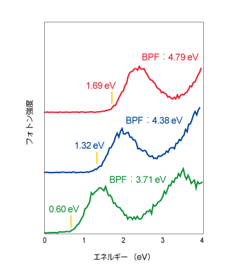
measured by replacing the bandpass filter
LEIPS spectra of a copper phthalocyanine thin film sample (10 nm deposited on ITO) measured by changing the bandpass filter (BPF)
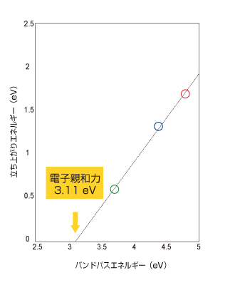
Plot of the onset energy of LEIPS spectra against the optical bandpass energy
Sample provided by: Center for Organic Photonics and Electronics Research for Practical Applications (i3-opera)
Low-damage analysis of organic materials
LEIPS achieves low-damage analysis of organic materials by using electrons of 5 eV or less as the primary probe. We present the results of long-duration LEIPS measurements on C60 thin films, along with LEIPS measurements acquired after irradiating with 10 eV electrons — equivalent to conventional inverse photoemission spectroscopy — for a fixed period. While LEIPS shows no change in spectral shape even after extended accumulation, a change in spectral shape is observed after 10 eV electron irradiation, demonstrating electron-induced damage.
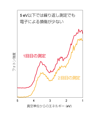
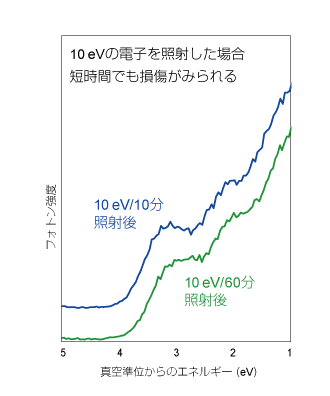
Sample provided by: Center for Organic Photonics and Electronics Research for Practical Applications (i3-opera)
Same-point analysis with LEIPS, XPS, and UPS
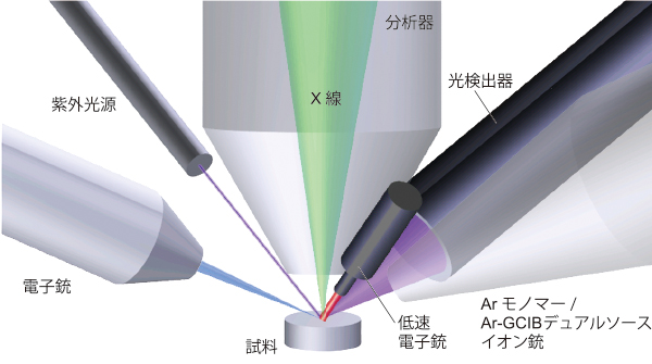
With PHI’s XPS instruments, the unique instrument configuration enables LEIPS, UPS, AES, REELS (Reflection Electron Energy Loss Spectroscopy), Ar cleaning, GCIB cleaning effective for organic materials, and charge neutralization — all to be performed at the same XPS analysis position. This makes it easy to achieve same-point irradiation with a variety of techniques, contributing greatly to comprehensive multi-faceted evaluation of samples.
Principles of LEIPS
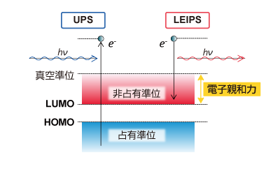
The energy diagram for semiconductor sample measurement by LEIPS and UPS is shown. LEIPS analyzes unoccupied states by measuring light (hν) generated upon electron (e⁻) irradiation. UPS, on the other hand, analyzes occupied states by measuring photoelectrons (e⁻) generated upon light (hν) irradiation. By reversing the roles of light and electrons, LEIPS enables direct measurement of properties such as electron affinity.
Features of LEIPS (GENESIS option)
LEIPS Measurement Method
*LEIPS: Low Energy Inverse Photoelectron Spectroscopy (1, 2, 3)
A schematic diagram of LEIPS is shown. The system consists of a low-energy electron gun, optical lens, bandpass filter, and photomultiplier tube.
The measurement method involves irradiating the sample with electrons at a fixed energy, while sweeping the bias voltage applied to the sample so that the irradiation energy is reduced to a low velocity of 0 to 5 eV.
Near-ultraviolet light generated from the sample is then detected by the photomultiplier tube through the optical lens and bandpass filter.
By selecting an appropriate bandpass filter, the energy range of the detected near-ultraviolet light can be changed.
From this information, it is possible to determine the value of the conduction band minimum referenced to the vacuum level and the electron affinity.
The vacuum level of the sample is defined as the position obtained by adding the bandpass filter energy to the onset position of the absorption current in the sample measured simultaneously with spectrum acquisition — that is, the position at which the kinetic energy of the incident electrons exceeds the vacuum level and current begins to flow.
Furthermore, since the photodetector is located on the atmospheric side, the bandpass filter used to select the light energy can be easily replaced.
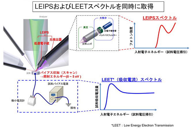
[Differences between LEIPS and conventional inverse photoemission spectroscopy instruments]
| Item | LEIPS | Conventional inverse photoemission spectroscopy instrument |
|---|---|---|
| Sample analysis position | Same-point analysis as XPS and UPS is possible Ar gun and GCIB gun can also irradiate at the same position | Analysis at a different position from XPS and UPS Sample transfer is required |
| Electron energy | 5 eV or below Low damage to organic materials | ~ 10 eV High damage to organic materials |
| Selection of light energy | Bandpass filter can be replaced in air | Practically impossible |
| Energy resolution | 0.45 eV or below | ~ 0.6 eV |
Method for determining electron affinity
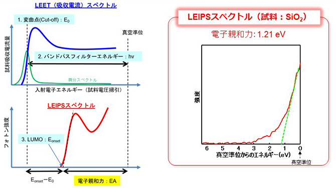
- Confirm the inflection point of the cut-off in the LEET spectrum (= the maximum point obtained by differentiating the spectrum)
- Determine the vacuum level from the photon energy hν (calculated from the center wavelength of the bandpass filter) referenced to the cut-off
- Onset of the LEIPS spectrum referenced to the vacuum level
(LUMO) position is calculated → Electron affinity is determined
Electron affinity can also be calculated from the following formula: EA = hν − (EOnset − E₀)
References
- H. Yoshida, Chem. Phys. Lett. 539-540, 180 (2012).
- H. Yoshida, J. Electron Spectrosc. Relat. Phenom. 204, 116 (2015).
- 吉田 弘幸,「 低エネルギー逆光電子分光装置の開発と有機エレクトロニクスへの応用」, 応用物理84(3), 245-249 (2015)
Patent:P6108361(固体の空準位測定方法及び装置:吉田 弘幸)
Related Instruments Links
X-ray Photoelectron Spectrometer XPS