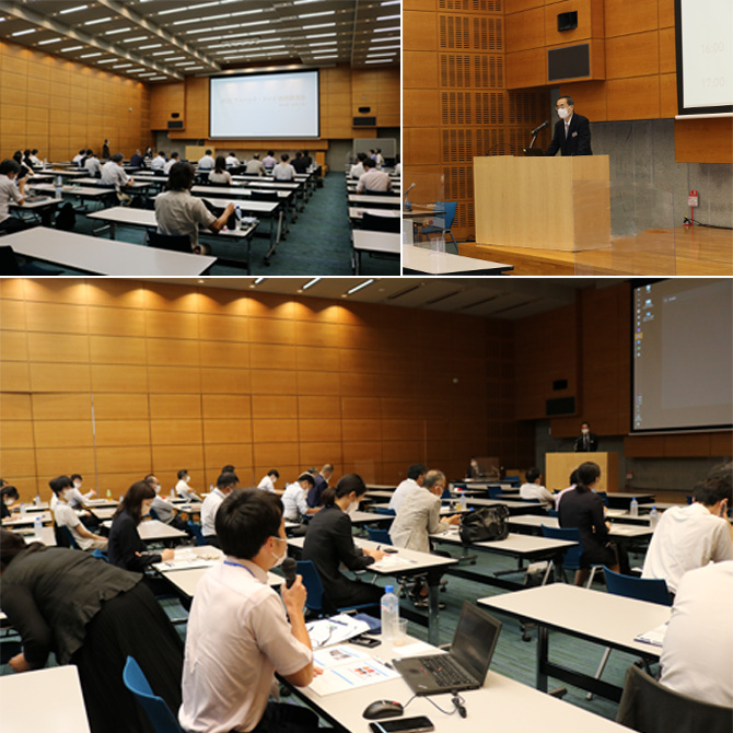
On Friday, July 8, 2022, we held our Technical Symposium at Architectural Institute of Japan Hall (Tamachi, Tokyo). Following the in-person event in 2019, we had been forced to hold the event online due to COVID-19, but this marked a return to an in-person venue for the first time in three years. As a COVID-19 precaution, the venue capacity was limited to 50 persons, with separate online viewing also made available. Attendees at the venue shared comments such as “I listened with great interest” and “I was able to broaden my perspective.” The web streaming was also viewed by many people.
We would like to once again express our sincere gratitude to Mr. Masaki Hachiya of Fujifilm Corporation, Mr. Jun Kimura of Sumitomo Electric Industries, Ltd., and Prof. Ryoji Kanno of Tokyo Institute of Technology (in order of presentation).
> Click here for the program on the day
Lectures
“Advancing the Development of High-Performance Materials through Surface and Interface Analysis”
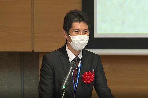
Mr. Masaki Hachiya
Analysis Technology Center, CTO Office, Fujifilm Corporation
Mr. Hachiya of Fujifilm Corporation delivered a lecture titled “Advancing the Development of High-Performance Materials through Surface and Interface Analysis,” covering the application of informatics to TOF-SIMS depth profiles and specific examples of the use of Ar-GCIB sputtering.
Regarding the application of informatics, examples of analyzing interfacially segregated components were presented, demonstrating the strengths of multivariate analysis using NMF (Non-negative Matrix Factorization).
Regarding the application of Ar-GCIB sputtering, two methods were introduced. First, regarding depth profiling by C60/Ar-GCIB co-sputtering, it was presented that simultaneous irradiation reduces organic damage and silica filler residue, thereby suppressing the unevenness seen during individual irradiation and achieving high resolution. Next, regarding the Ar-GCIB sputter collection method, specific examples were used to describe cases in which only the components within the surface 30 to 50 nm of a polymer thin film were successfully collected and analyzed. In particular, the story of using a mechanical watch to automatically rotate the sample and thereby improve collection efficiency was very interesting and impressive.
It was also emphasized that taking ownership of development and manufacturing challenges — treating them as “one’s own” — is important in addressing various issues. It was a lecture that was not only technically informative but also very educational in terms of attitude toward work.
“The Role of an In-House Analysis Division — The Case of Sumitomo Electric”
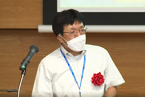
Mr. Jun Kimura
Center Director, Analysis Technology Research Center, Sumitomo Electric Industries, Ltd.
Mr. Kimura of Sumitomo Electric Industries, Ltd. spoke from his position as Center Director of the Analysis Technology Research Center about the company’s history starting from copper, the five business fields (automotive, information and communications, electronics, environmental energy, and industrial materials) that support today’s Sumitomo Electric — developed through the technologies cultivated along the way — and the relationship between these business fields and the research, development, and analysis teams that support them.
Drawing on a phrase from Sumitomo Electric’s public relations magazine — that analysis is the challenging task of “making the invisible visible” — Mr. Kimura explained using clear examples how the analysis and characterization division addresses this challenge.
In particular, from the perspective of recovering analysis costs, we were able to clearly understand how quantifying the value that the analysis division provides to company executives and personnel at all levels has contributed to the development of the company and its Analysis Center today.
Regarding the suggestions for future analytical technologies — including computational science, automation, large-scale data, and digital analysis — we at the analytical instrument manufacturer listened while thinking about how we could break down these keywords and present new useful tools to the world. It seemed that the audience at the venue felt a sense of empathy from the perspective of an analysis center, and gained many learnings from the perspective of organizational management.
“All-Solid-State Batteries — Challenges and Science”
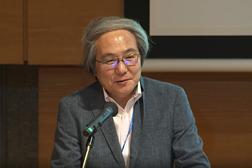
Prof. Ryoji Kanno
Center Director, All-Solid-State Battery Research Center
Institute of Innovative Research, Tokyo Institute of Technology
Prof. Ryoji Kanno of Tokyo Institute of Technology is a researcher of world renown for his pioneering research on all-solid-state battery materials. At the Technical Symposium, he delivered a lecture titled “All-Solid-State Batteries — Challenges and Science,” and we had the very valuable opportunity to hear directly from Prof. Kanno himself about the history of storage batteries, the characteristics of all-solid-state batteries, and research related to exploring the present and future of all-solid-state batteries.
Through the process of clarifying the challenges of materials exploration aimed at achieving all-solid-state batteries in the future, we were able to learn in detail about the circumstances that led to the discovery of the superionic conductor Li10GeP2S12 (referred to as LGPS) — found by searching for solid electrolytes in which ions can move at high speed within a solid — and about the current state of progress that has brought the practical realization of all-solid-state lithium batteries significantly closer.
The research content was deeply impressive — exploring the crystal structures of various ion conductors based on the belief that a successful material always exists near the one being targeted, discovering new materials, and ultimately prompting the emergence of a new category of devices. We believe many attendees were deeply moved by this. All-solid-state battery technology, which can only be realized through the comprehensive optimization of the combination of electrode materials and electrolyte materials and their interface formation technology, is regarded as the ideal form of a chemical-electrical energy conversion device, and great expectations are being placed on it as a future technology.
Thank you very much for the invaluable lectures.
From ULVAC-PHI
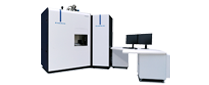
Our Product Strategy Department presented our new XPS product “PHI GENESIS.”
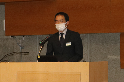
This was followed by a presentation from our Solution Development Department introducing “Imaging of Buried Interfaces by PHI nanoTOF 3 FIB-TOF.”