PHI 710
Scanning Auger Electron Spectrometer (AES/SAM)
The PHI 710 Scanning Auger Electron Spectrometer is the world's only Auger analyzer guaranteed to deliver an Auger electron spatial resolution of 8 nm or better. Equipped as standard with an acoustic enclosure, it enables low-drift Auger analysis at 500,000× magnification — a condition previously unattainable with conventional Auger systems — achieving true nanometer-level microarea Auger analysis.
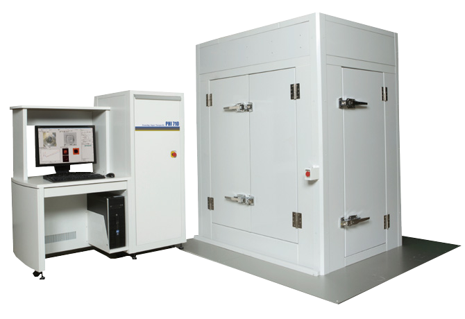
SEM resolution ≤ 3 nm, AES resolution ≤ 8 nm
In Auger analysis (spectrum, depth profile or mapping), it is necessary to set AES analysis point with SEM image. A fine focused electron beam is required for SEM imaging and an extremely stable electron beam at enough current for AES analysis is required at a time. PHI 710 provides < 3 nm of SEM spatial resolution by reducing the noise from power supply.
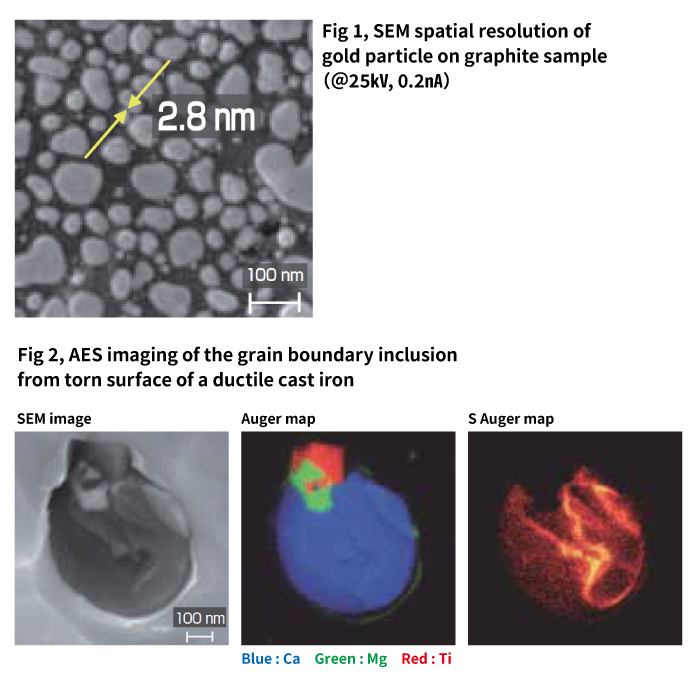
AES spatial resolution reached to < 8 nm (@ 20 kV, 1 nA) by adopting an acoustic enclosure box, which minimizes the effect of vibration, sound, and temperature change (Fig.1).
Fig. 2 shows imaging of the grain boundary inclusion from torn surface of a ductile cast iron. A secondary electron image (left), overlaid Auger mapping image for Ca, Mg, & Ti (center), and sulfur Auger mapping image(right) are shown.
High sensitivity/high throughput analysis with coaxial cylindrical mirror analyzer (CMA)
Coaxial cylindrical mirror analyzer
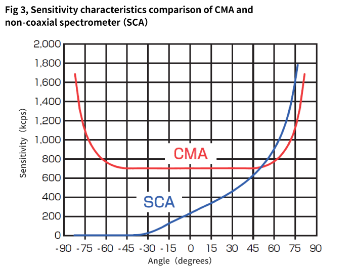
Coaxial CMA (Cylindrical Mirror Analyzer) is PHI’s unique electron spectrometer which has the electron gun on the central axis of it. CMA has a strong advantage of making less likely to be affected by sample shape or tilt angle, because CMA can capture Auger electron emitted in 360 degrees from the sample. Fig. 3 shows the difference of sensitivity characteristics between coaxial CMA and non-coaxial spectrometer (SCA). CMA has high sensitivity characteristic from vertical incidence to oblique incident, while achieving a flat sensitivity characteristic with low angle dependence. Therefore PHI 710 can provide superior quantitative data at various incidence angles and sample shapes.
Various shapes of samples are supported
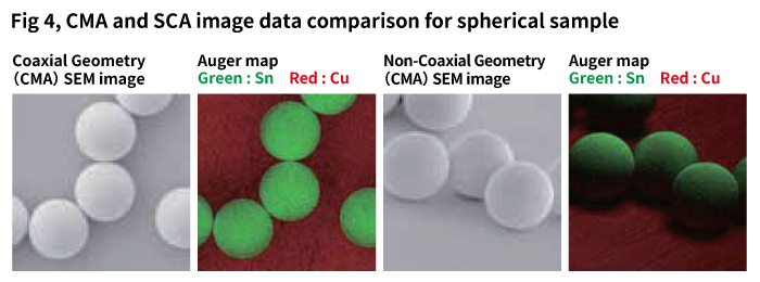
Fig. 4 shows the comparison of CMA and SCA by SEM image and Auger mapping image of Sn balls on Cu. While Auger mapping image by SCA shows a significant shadow effect, Auger mapping image by CMA is clearly corresponding with the SEM image without shadow, providing accurate understanding of sample.
Chemical state mapping by AES
Spectrum mapping
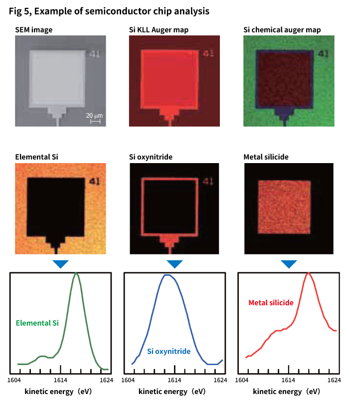
PHI 710 can get spectrum mapping data in Auger mapping analysis, which maintains the spectrum for each pixel. This function provides a chemical state mapping image based on spectral analysis from each pixel.
High energy resolution Auger map
Fig. 5 shows results of Si KLL spectrum mapping measurement of a semiconductor chip electrode. Applying Linear Least Squares Fitting (LLS) data process to the Si KLL spectrum, mapping image clearly shows the three separated areas consisting of elemental Si, Si oxynitride, and metal silicide. Lower column shows the Si KLL spectrum extracted from the map data, for each of the three states.
AES Related Information
CONTACT
Feel free to contact us with any questions about our products, analysis services, or careers.